

Items : %s%s


LCMXO640C-4MN132I

LCMXO640C-4MN132I
477-LCMXO640C-4MN132I
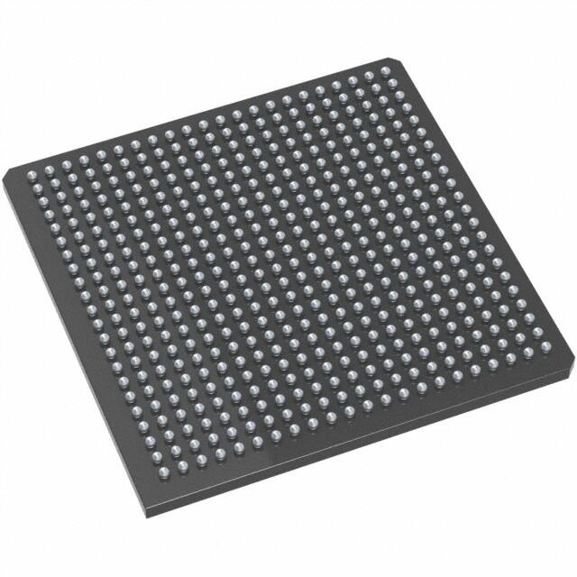
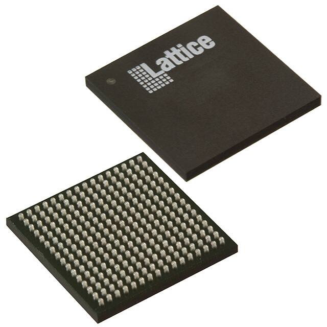
132-LFBGA, CSPBGA
3.3V V 1.35mm mm 4.2 ns ns FPGAs MachXO Series 132-LFBGA, CSPBGA 17mA mA 0.5mm mm 132
In Stock : 999
Share
Please send RFQ, we will respond immediately.


Product Details
Purchasing and Inquiry
LCMXO640C-4MN132I Overview
There are two packages that contain fpga chips: 132-LFBGA, CSPBGA package and X package. FPGAs of this type consist of FLASH PLD components. Its 101 I/Os help it transfer data more efficiently. The basic building blocks of logic contain 640 logic elements/cells. Fpga chips is powered from a supply voltage of 1.8V. An FPGA part from the Field Programmable Gate Arrays family. With a Surface Mount connector, this FPGA module can be attached to the development board. Fpga chips operates wFpga chipsh a supply voltage of 1.71V~3.465V. The MachXO series FPGA is a type of FPGA that belongs to the MachXO family of FPGAs. Fpga chips is necessary to keep the operating temperature wFpga chipshin -40°C~100°C TJ when the device is operating. In this device, 101 outputs are incorporated in order to provide you with maximum flexibility. Fpga chips is designed to maximiTraye space efficiency by containing the FPGA model in Tray. In total, the terminations of this piece are 132. Related parts can be found by using its base part number LCMXO640. The RAM si0Be of this FPGA module reaches 0B so as to guarantee the normal operation of the program during operation. Fpga electronics is designed wfpga electronics h 132 pins. This FPGA is built as an array of 80 LABs/CLBs. I think, as long as this FPGA is mounted in Surface Mount, it could perform excellently according to its specifications as long as you mount it in Surface Mount. In operation with 3.3V, designers can take advantage of its flexibility to the fullest extent. A total of 132 pins are included in this device. Fpga semiconductor is possible for this FPGA to reach speeds of up to 550MHz. It incorporates 640 logic cells used for the building block. It operates at 17mA amps of supply current. A feature of this system is also called IT CAN ALSO OPERATE AT 2.5V AND 3.3V, which gives it a unique characteristic. To determine the status of the input signals, 7 dedicated inputs are available in the system. The main building blocks of a CPLD can be found in this device, namely 320 macro cells. The SRAM memory is optimiSRAMed for data storage and resource management.
LCMXO640C-4MN132I Features
101 I/Os
132 LABs/CLBs
LCMXO640C-4MN132I Applications
There are a lot of Lattice Semiconductor Corporation LCMXO640C-4MN132I FPGAs applications.
- Cryptography
- Medical imaging
- Audio
- Device controllers
- Military Temperature
- Secure Communication
- Software-defined radios
- Integrating multiple SPLDs
- Automotive
- Medical ultrasounds
You can send an inquiry by email, or add the item to the RFQ list and submit it to us.
Tell us the model and quantity you need, our sales staff will reply the price in time.
 Email for receiving inquiries: jindawei@hkjdwchip.com
For your convenience, we accept multiple payment methods in USD, including PayPal, Credit Card, and wire transfer.
3. RFQ (Request for Quotations)It is recommended to request for quotations to get the latest prices and inventories about the part.
Our sales will reply to your request by email within 24 hours.
1. You'll receive an order information email in your inbox. (Please remember to check the spam folder if you didn't hear from us).
2. Since inventories and prices may fluctuate to some extent, the sales manager is going to reconfirm the order and let you know if there are any updates.
Shipping starts at $40, but some countries will exceed $40. For example (South Africa, Brazil, India, Pakistan, Israel, etc.)
The basic freight (for package ≤0.5kg or corresponding volume) depends on the time zone and country.
Currently, our products are shipped through DHL, FedEx, SF, and UPS.
Delivery TimeOnce the goods are shipped, estimated delivery time depends on the shipping methods you chose:
FedEx International, 5-7 business days.
The following are some common countries' logistic time.
Payment Method
| The fee is charged according to the rule of PayPal. | |
| East West Bank charge US$30.00 banking fee. | |
| The fee is charged according to the rule of PayPal. | |
| Western Union charge US$0.00 banking fee. |
Shipping
| DHL(www.dhl.com) From $40.00 basic shipping fee depend on zone and country. |
|
| UPS(www.ups.com) From $40.00 basic shipping fee depend on zone and country. |
|
| FedEx(www.fedex.com) From $40.00 basic shipping fee depend on zone and country. |
|
| Registered Mail(www.singpost.com) From $10.00 basic shipping fee depend on different zone and country. |
Package
|
|
|
|
|
|
LCMXO640C-4MN132I
technical specifications, attributes, parameters and parts with similar specifications to LCMXO640C-4MN132I.
Hot Sales in Thermal
.png)


Parts with Similar Specs
The three parts on the right have similar specifications to Aavid.
-
ImagePart NameManufacturerHK JDW NOPackageStockDataSheet:Compare:
-
 Lattice Semiconductor Corporation477-LCMXO2-2000HC-4TG144I144-LQFP2-3 DaysAdd Compare
 -
 Lattice Semiconductor477-LCMXO2-1200ZE-1MG132I132-LFBGA, CSPBGA2-3 DaysAdd Compare
 -
Lattice Semiconductor477-LCMXO2-256ZE-1MG132C132-LFBGA, CSPBGA2-3 DaysAdd Compare
-
Lattice Semiconductor Corporation477-LCMXO2-1200HC-4TG144I144-LQFP2-3 DaysAdd Compare
-
 Lattice Semiconductor Corporation477-LCMXO2-1200HC-4TG100C100-LQFP2-3 DaysAdd Compare
 -
Lattice Semiconductor477-LCMXO256C-3TN100I100-LQFP2-3 DaysAdd Compare
-
 Lattice Semiconductor477-LCMXO2-2000ZE-1BG256C256-LFBGA2-3 DaysAdd Compare
 -
Lattice Semiconductor477-LCMXO2-2000ZE-1BG256I256-LFBGA2-3 DaysAdd Compare
 Need Help?


