IMEC and ASML collaborate: Breakthroughs in High-NA EUV technology in logic and DRAM patterning

In the field of semiconductor technology, the progress of extreme ultraviolet lithography (EUV) technology has always attracted much attention. Recently, the collaboration between imec and ASML marked an important milestone: the successful patterning of logic and DRAM structures using ASML’s High-NA EUV technology. This achievement not only demonstrates the application of cutting-edge technology, but also heralds the future trend of semiconductor manufacturing.
Advantages of High-NA EUV Technology
High-NA EUV technology, with its higher numerical aperture, can significantly improve the resolution of patterns. This means chipmakers can implement more complex circuit layouts on the same silicon area, thereby increasing chip performance and density. This technology breaks through the limitations of traditional EUV lithography, making it possible to achieve precise patterning on a smaller scale.

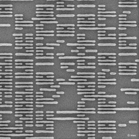
▲ 2D features Image source: imec, same below

▲ Dense metal wire.
Applications in logic and DRAM
In logic chip manufacturing, High-NA EUV technology makes it possible to achieve higher levels of integration, which is critical to meeting future computing needs. For DRAM (Dynamic Random Access Memory), smaller pattern size not only increases storage density, but also improves access speed and energy efficiency, thus driving higher performance memory solutions.
The significance of technological breakthroughs
This technological breakthrough has far-reaching consequences. First, it demonstrates the central role of EUV technology in achieving the goals of next-generation semiconductor technology. Secondly, successful patterning applications provide new possibilities for future chip manufacturing, further promoting the progress of Moore's Law. The maturity of High-NA EUV technology is expected to lead the semiconductor industry into a new technology era.
future outlook
With the advancement of High-NA EUV technology, chip manufacturers can achieve higher integration and performance on a smaller scale. This not only has an important impact on logic chips and DRAM, but also lays the foundation for various high-tech applications. In the future, we can look forward to the application of this technology in a wider range of semiconductor fields, including advanced sensors, communication equipment, and artificial intelligence computing platforms.
Overall, the cooperation between imec and ASML marks a major advancement in semiconductor manufacturing technology and heralds a new era full of innovation and challenges. As technology continues to evolve, we have reason to believe that this breakthrough will bring more exciting developments to the semiconductor industry.


 Need Help?


