The 555 timer is an integrated circuit (IC) widely used in electronics to generate precise timing pulses. The 555 timer is commonly used in applications such as timers, oscillators, pulse generators, and waveform shaping circuits.
Electronics Basics: Introduction to the 555 Timer IC
Let us understand the 555 timer through the following points
| · 555 Timer Design |
| · 555 Timer Pinout |
| · Internal Structure and Diagram of 555 Timer |
| · What is 555 Timer Used for? |
| · 555 Timer Parameters |
| · Derivative chip of 555 timer |
555 Timer Design
Introduced by Signetics (now ON Semiconductor) in 1972, the 555 timer has a fascinating design history. Designed by Swiss-American electronics engineer Hans R. Camenzind, it is a simple yet versatile integrated circuit (IC) capable of generating precise timing signals for a variety of electronic applications.
Prior to 1972, timer circuits typically required the use of a large number of discrete components such as transistors, capacitors, and resistors to implement specific time delay and pulse control functions. This not only leads to an increase in circuit complexity and cost, but is also prone to problems in the design process. The emergence of the 555 timer chip has completely changed this situation.
Kamenzinde's designs were revolutionary for their time. It combines a pair of comparators, a voltage divider network, and a flip-flop circuit in one package. This arrangement allows the 555 timer to operate in several modes, including astable (continuous oscillation), monostable (single-stable pulse generation), and bistable (flip-flop).
In 1972, Signetics released the first 555 timer IC in 8-pin DIP and 8-pin TO5 metal can packages, namely SE/NE555 timer, which was the only commercial timer IC at that time.
The NE555 has an operating temperature range of 0-70°C, and the military-grade SE555 has an operating temperature range of −55 to +125 °C. The package of 555 is divided into high-reliability metal package (indicated by T) and low-cost epoxy resin package (indicated by V), so the complete labels of 555 are NE555V, NE555T, SE555V and SE555T. It is generally believed that the source of the name of the 555 chip is the three 5KΩ resistors, but Hans Camenzind denied this statement and claimed that he took these three numbers at will.

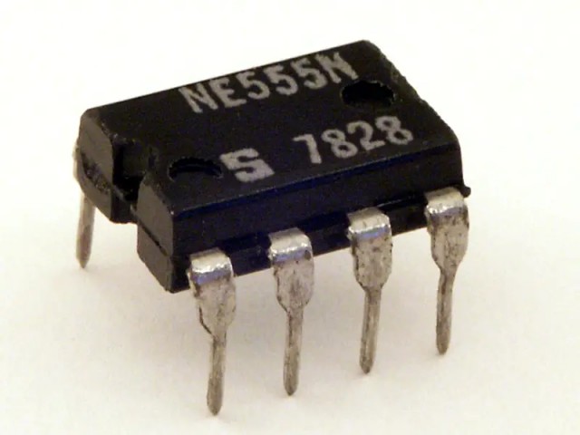
NE555N Timer Image
Today, many manufacturers produce 555 timers, including bipolar traditional models transistors and versions designed in CMOS. The 555 timer is considered to be one of the chips with the highest output in the world. According to statistics from 2003 to 2017, the annual output is as high as 1 billion!
The 555 chips produced by different manufacturers have different structures. The standard 555 chip integrates 25 transistors, 2 diodes and 15 resistors and leads out through 8 pins (DIP-8 package). Derivatives of the 555 include the 556 (which integrates two 555 DIP-14 chips) and the 558 and 559
There are also low-power versions of the 555, including the 7555 and the TLC555 using CMOS circuits. The power consumption of the 7555 is lower than that of the standard 555, and its manufacturer claims that the control pin of the 7555 does not require a grounding capacitor like other 555 chips, and at the same time There is also no need for decoupling capacitors between the power supply and ground to eliminate noise.
555 Timer Pinout
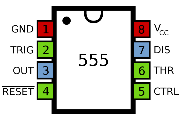
The standard 555 chip is a DIP-8 package with eight pins, as follows,

555 Timer Pinout
Each pin is explained in detail below:
Pin | Name | Features |
1 | GND (ground) | Ground, as a low level (0V) |
2 | TRIG(trigger) | When the voltage of this pin drops to 1/3VCC (or the threshold voltage determined by the control terminal), the output terminal gives a high level. |
3 | OUT (output) | Output high level (+VCC) or low level. |
4 | RST (reset) | When this pin is connected to high level, the timer works, and when this pin is connected to ground, the chip resets and outputs low level. |
5 | CTRL (control) | Controls the threshold voltage of the chip. (When this pin is empty, the default two threshold voltages are 1/3VCC and 2/3VCC). |
6 | THR (threshold) | When the voltage of this pin rises to 2/3VCC (or the threshold voltage determined by the control terminal), the output terminal gives a low level. |
7 | DIS (discharge) | The OC gate is internally connected to discharge the capacitor. |
8 | V +, VCC (power) | Provide high level and power the chip. |
When using a 555 timer chip, these pins need to be properly connected depending on the desired function and application. For example, in monostable mode, the TRI pin is usually connected to the trigger input through an external component, the OUT pin is used to output a pulse signal, and the RST pin can be used for reset operation.
It should be noted that the pin configuration may vary depending on the package type of the chip. Therefore, when using a specific model and package of 555 timer chips, you should refer to the relevant data sheet and specification sheet for the correct pin configuration information.
Internal Structure and Diagram of 555 Timer
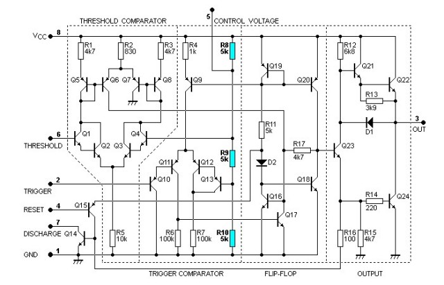
The standard 555 is composed of 25 transistors, 2 level tubes, and 15 resistors. The internal schematic diagram of the chip is as follows,

555 Timer Circuit Schematic Diagram
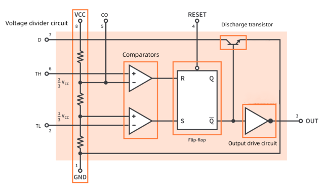
For the convenience of understanding, we can divide it into several basic functional modules, as shown below,

555 Timer Internal Block Diagram
Voltage divider circuit:The voltage divider circuit of the first part of the block diagram, the voltage divider consists of 3 5k resistors. Since these 3 resistors have the same value, an equal voltage is distributed between these 3 resistors and the voltage across the resistors acts as a reference voltage for the comparator.
CONTROL is connected between the upper two resistors to allow an external voltage to control the reference voltage:
When CONTROL is not driven, the divider produces an upper reference voltage of 2⁄3 VCC and a lower reference voltage of 1⁄3 VCC.
When CONTROL is driven, the upper reference voltage will be VCONTROL and the lower reference voltage will be 1⁄2 VCONTROL.
Comparator:comparator is a type of operational amplifier. The comparator mainly compares the voltage of the input terminal, and outputs a high voltage or a low voltage according to the higher voltage of the inverting input or the non-inverting input.
1) The input of the upper comparator (threshold comparator) is the threshold pin connected to the non-inverting input (+), and the reference voltage of 2/3Ucc is connected to the inverting input (-) of the comparator. Another external pin "Control Voltage" is connected to the inverting input (-) of this comparator, so that you can override the reference voltage of 2/3Ucc and also change the width of the output signal.
2)2) For the comparator below (trigger comparator) 1/3 Ucc reference voltage is supplied to the non-inverting input (+) and the trigger pin is connected to the inverting input (-) of the comparator.
The output of the comparator serves as the input of the flip-flop. The SR flip-flop is a storage element that can store and output logic "0" or logic "1" according to two inputs SEF and RESET or S and R, respectively. The outputs of the flip-flops are Q and Q BAR , where Q and Q BAR are complementary sets.
The output of the flip-flop is supplied to the output driver circuit to increase the current level, and finally passed to the external output pin of the IC.
Flip-Flop: The 555 timer contains an SR (Set-Reset) flip-flop that is controlled by the comparators. Depending on the voltage levels detected by the comparators, the flip-flop is set or reset, leading to changes in the output state.
Discharge Transistor: The 555 timer includes an internal discharge transistor connected to the discharge pin (pin 7). This transistor is used in certain modes to discharge an external capacitor, affecting the timing characteristics of the circuit.
Voltage Comparator: The voltage comparators within the 555 timer determine whether the voltage at the Threshold pin is greater or less than the voltage at the Trigger pin. The output of these comparators affects the state of the internal flip-flop.
What is 555 Timer Used for?
The 555 timer serves three different purposes. The 555 timer can be configured in various modes such as astable, monostable and bistable, which determine its behavior. Here is a brief overview of these modes:
Astable Mode: In this mode, the 555 timer operates as an oscillator, producing a continuous square wave output. The frequency and duty cycle of the output waveform can be controlled using external resistors and capacitors.
Monostable Mode: In Monostable mode, the 555 timer acts as a monostable pulse generator. It generates a single pulse of specified duration in response to a trigger signal. This mode is commonly used in applications such as timers, delay circuits, and pulse width modulation.
Bistable Mode (or Schmitt Trigger Mode): Bistable mode turns the 555 timer into a flip-flop or toggle switch. It has two stable states and can be switched between them using an external trigger signal. This mode is typically used in applications such as simple latch circuits and control systems.
Parameters of 555 Timer
The following are the electrical parameters of NE555, other 555 timers with different specifications may have different parameters, please refer to the data sheet.
Derivative Chip of 555 Timer
The 555 timer has many derivative models produced by different companies, including models with different pin functions and CMOS designs. Some chips include several integrated 555 timers. Some other models of the 555 chip family are as follows:
Mfr | Mfr No | Note |
Avago Technologies | Av-555M | |
Custom Silicon Solutions | CSS555/CSS555C | CMOS, Minimum working voltage 1.2V, IDD<5µA |
CEMI | ULY7855 | |
ECG Philips | ECG955M | |
Exar | XR-555 | |
Fairchild Semiconductor | NE555/KA555 | |
Harris | HA555 | |
IK Semicon | ILC555 | CMOS, Minimum working voltage 2V |
Intersil Corporation | SE555/NE555 | |
Intersil Corporation | ICM7555 | CMOS |
Lithic Systems | LC555 | |
Meixin | ICM7555 | CMOS, Minimum working voltage 2V |
Motorola | MC1455/MC1555 | |
NTE Sylvania | NTE955M | |
RCA | CA555/CA555C | |
STMicroelectronics | NE555N/ K3T647 | |
TI(Texas Instruments) | SN52555/SN72555 | |
TI(Texas Instruments) | TLC555 | CMOS, Minimum working voltage2V |
Zetex | ZSCT1555 | Minimum working voltage 0.9V |
NXP | ICM7555 | CMOS |
HFO | B555 | |
HITACHI | HA17555 |
556 Dual Timer
The model that integrates two 555 timers in one chip is 556, and this chip includes 14 pins.
558 four timer
The model that integrates four 555 timers in one chip is 558. This chip includes 16 pins, among which four 555 timers share power supply, ground and reset pins. The discharge pin and the threshold pin are combined into one pin and called "timing". At the same time, the trigger pin is changed to a falling edge trigger.


 Need Help?


